Integrated Clock Gating Cell

Clock gating is a common technique for reducing clock power by shutting off the clock to modules by a clock enable signal.Clock gating functionally requires only an AND or OR gate. Consider you were using an AND gate with clock. The high EN edge may come anytime and may not coincide with a clock edge. In that case the output of the AND gate will be a 1 for less time than the clock’s duty cycle. You in turn end up with a glitch in your clock signal.

To avoid this, a special kind of clock gating cells are used, that synchronizes the EN with a clock edge. These are call integrated clock gating cells or ICG.

There are two commonly used ICG cell types.

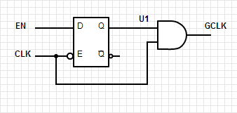
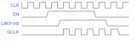
  • Using AND gate with high EN
    The following design uses a negative edge triggered latch to synchronize the EN signal to the CLK. The GCLK is available only when the latch o/p is high. GCLK is held low when EN is low.

    ICG_AND
    AND_ICG_tim

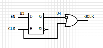
  • Using OR gate with high EN

    The following design uses a positive edge triggered latch. GCLK is held high when EN is low.Note that the latch o/p is inverted at the OR input. Hence, the clock is passed through when this i/p gets a low.

    ICG_OR

    OR_ICG_tim

17 comments on “Integrated Clock Gating Cell

  1. pramod

    How timing checks are done on reg to clg paths? Why there are two setup time(clk gating and nochange) and two hold times are coming for this path? Can you please tell me?

    Reply
  2. Anil

    Hi Sini ,

    Does Latch o/p waveform delayed by 1 clock cycle compare to enable though it is level sensitive latch? If so what is the reason?

    Regards,
    Anil

    Reply
    1. Sini

      It wont be held another one cycle, but if the change occurred when the clock was not active, it will be held. I think the timing diagrams are a bit off. Assume the EN going low after the negative edge of the clk in the last timing diagram above.

      Reply
  3. ethan

    Hi, sini,
    I got some questions about ICG,

    In posedge synchronous design, we often use AND gate with high EN.
    But the clock is held low when enable is low. Posedge FFs constitute of two latchs, clk = 0 makes the first latch toggle all the time.
    How can this power saved?

    Regards,
    ethan

    Reply
  4. Sangeetha

    Is “OR” gate based clock gating used only when driving a negative edge triggered flip flop and “AND” gate based clock gating only used for positive edge triggered flip-flops?

    Reply
  5. Sarath Chandra

    Hi sini,
    How come edge trigger word is used in latches?For latches it should be level triggered.
    Hope my question is a valid one.

    Reply
    1. Sini Mukundan Post author

      In common usage yes. But flip flop is also an edge sensitive latch. This is the nomenclature usually used for ICG cells, as one is an enable signal.

      Reply
  6. nirmal

    Hi Sini
    In AND based clock gating, there is a possibility of clock pulse cut off before clock period. But in latch based clock gating, there is a possibility of losing a clock pulse entirely if latch setup timing is violated(meaning lath enable comes just after clock edge). Am i right?

    Reply
  7. Ajay Gudi

    Hi ,
    Can you let me know how much will be fanout limit for the ICG and what should be the bit width limit also for inserting ICG.

    What is the use of inserting control point before and after the ICG ?

    Thanks
    Ajay Gudi

    Reply
  8. Sethiya

    Hi,
    I want to know, will it make a difference between, when we use a descrete “Latch & an AND” gate for clock gating vs a ICG cell from library?

    Reply
  9. Badarinath Gopalakrishna

    suppose there is a glitch of time period less than half of the clk period occuring during the negative half of the clock, the latch will be transparent and will simply transfer the glitch right?

    Reply
  10. Ashikur Rahman

    Thank You , for such a well described article . But , most of the cases I have found a latch in the place of flip flop over the different blog and in some reading material .In my opinion it also make sense to use latch ,as our desire target is to block transition in “En” pin at low or high level . So, if latch is used instead of flip flop or vice versa, then what will be the impact ?

    Reply
  11. Pingback: Clock Gating Checks – VLSI Pro

Leave a Reply

Your email address will not be published. Required fields are marked *