Physical Design Flow I : NetlistIn & Floorplanning
This is going to be a series of step-by-step explanation of physical design flow for the novice. I am going to list out the stages from Netlist-GDS in this session. Of course some say synthesis should also be part of physical design, but we will skip that for now.
So, you have completed your RTL, synthesised it and now you have a netlist & constraints. Next comes the physical design part of it;making your design into a representation of the actual geometries you will manufacture. You will do a bunch of stuff here, like floorplanning, placement, CTS, routing, timing closure, physical verification, formal verification etc. The major stages are explained below.
Netlist In
The first stage in physical design flow is reading in the netlist and the constraints to your tool of choice. Let us see what kinds of files we are dealing with here. I have used both Cadence and Synopsys tools extensively, so those are what I will base my examples on. However, every tool uses pretty much the same flow and even the same format files.
Gate Level Netlist
Once you choose a process and a library, a synthesis tool will translate your RTL into a collection of interconnected logic gates that define the logic. The most common format is verilog. I had seen some VHDL and EDIF designs when I started my career, but I have only really worked with Verilog files.Standard Cell Library
In digital design, you have a ready made standard cell library which will be used for synthesis and subsequent layouts. Your netlist will have instantiation of these cells. For digital layout, you need layout and timing abstracts for these cells.- Layout Model - An abstract model of the standard cell layout is used instead of the complete layout. This will have PINs defined, so as to facilitate automatic routing by the tool as per your netlist. Synopsys tool ICCompiler use "FRAM" views as a PnR abstract. FRAM view is a cell view that has only the PINs and metal and via blockages defined. This makes sure that the interconnection between the PINs can be routed automatically and that the routing tool will not route over existing metal/via areas thus ruling out any shorts. Cadence EDI tools use LEF views, which again has only the PINs and Obstructions (blockages) defined. LEF is an ascii file, so go ahead and have a read.
- Timing Model - Tools also need a timing model in the form of a .lib file. ICC takes a .db file, which is generated from a .lib. This liberty format file will have timing numbers for the various arcs in a cell, generally in a look up model. Please note that .libs may also have cell power information.
Technology File
The rules pertaining to the process you have selected should also be given to the PnR tool. This includes metal widths, spacing, via definitions etc. ICC takes a milkyway techfile format, while EDI tools take a technology LEF file. Please see this post for some details.Timing Constraints
SDC files define the timing constraints of your design. You will have the clock definitions, false paths, any input and output delay constraints etc.
These inputs once read in, will get you started with your database.
set search_path "<.db_file_paths>"
set link_library "\* std_lib1.db std_lib2.db"
create_mw_lib my_design_lib \
  -technology  \
  -mw_reference_library " \
  -open
read_verilog ./my_design.v
current_design
link
read_sdc
The above snippet of code creates a library with the name "my_design_lib". The .db files are specified using "set link_library" and the paths where they can be found at "set search_path".
Floorplanning
This is the first major step in getting your layout done, and for me this is the most important one.Your floorplan determines your chip quality.At this step, you define the size of your chip/block, allocates power routing resources, place the hard macros, and reserve space for standard cells.Every subsequent stage like placement, routing and timing closure is dependent on how good your foorplan is. In a real time design, you go through many iterations before you arrive at an optimum floorplan.
- Core Boundary
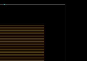
Floorplan defines the size and shape of your chip/block. A top level digital design will have a rectangular/square shape, whereas a sub block may have rectangular or rectilinear shapes. Core boundary refers to the area where you will be placing standard cells and other IP blocks. You may have power routing spaces allocated outside the core boundary. For a full chip, you will also have IO buffers and IO pads placed outside the core boundary.
In your PnR tool, floorplanning can be controlled by various parameters:
- Aspect ratio: This is the ratio of width divided by height and determines whether you get a square or rectangular floorplan. An aspect ratio of 1 gives you a square floorplan.
- Core utilization
Core utilization = (standard cell area+ macro cells area)/ total core areaA core utilization of 0.8 means that 80% of the area is available for placement of cells, whereas 20% is left free for routing. - Boundary: You can specify a boundary and ask the tool to honour it. This can come in handy when you have an existing boundary from a previous version.When you specify Boundary as the control parameter, both aspect ratio and core utilization are irrelevant. The tool gives you a report of the utilization for the current boundary specified.
read_pin_pad_physical_constraints ./pins.tdf
set_fp_pin_constraints -hard_constraints {layer location}  -block_level

read_def ./boundary.def

create_floorplan -control_type boundary -start_first_row -flip_first_row \
              -left_io2core 10 -bottom_io2core 10 \
-right_io2core 10 -top_io2core 10- IO Placement/Pin placement
If you are doing a digital-top design, you need to place IO pads and IO buffers of the chip.Take a reactangular or square chip that has pads in four sides.To start with, you may get the sides and relative positions of the PADs from the designers. You will also get a maximum and minimum die size according to the package you have selected. To place IOs, I use a perl script to place them once I decide on my chip size.
If you are doing a digital block, you will need to place pins around the boundary to connect to the higher level routing. Cadence tools can use a DEF file or a custom floorplan file to do this. ICC can read in a DEF or a pin placement file to do the SAME.
DEF extract:
DESIGN my_design_lib; UNIT DISTANCE MICRON 1000 ; DIEAREA ( 0 0 ) ( 1914800 1150100 ) ;

PINS 550 ; - sel\[1\] + NET sel\[1\] + DIRECTION INOUT + LAYER MET3 ( 0 0 ) ( 500 500 ) + PLACED ( 0 265900 ) N ; .... END PINS;

END DESIGN;- Macro placement Once you have the size & shape of the floorplan ready and initialized the floorplan, thereby creating standard cell rows, you are now ready to hand place your macros. Do not use any auto placement, I have not seen anything that works. Flylines in your tool will show you the connection between the macros and standard cells or IOs.
- Use flylines and make sure you place blocks that connects to each other closer
- For a full-chip, if hard macros connect to IOs, place them near the respective IOs
- Consider the power straps while placing macros. You can club macros/memories
Creating Power Rings and Straps
This is a topic worthy of its own article, and I will get to arriving at the number and width of power rings & straps in another post. Let me just now touch upon how to generate the power rings using ICCompiler. At this stage, you decide on the trunks that supply power to the core. You also have to make sure that all the hard macros have sufficient rings/straps around it to hook into the PG trunks. As usual, a robust power structure will take iterations and IR drop analysis at a later stage, but a close approximation can be arrived at the initial stages.
create_rectangular_rings, create_rectilinear_rings and create_power_straps are some commands in ICCompiler that will let you create the power network.