I. NetlistIn & Floorplan
II. Placement
III. Clock Tree Synthesis
After CTS, the routing process determines the precise paths for interconnections. This includes the standard cell and macro pins, the pins on the block boundary or pads at the chip boundary. After placement and CTS,the tool has information about the exact locations of blocks, pins of blocks, and I/O pads at chip boundaries. The logical connectivity as defined by the netlist is also available to the tool. In routing stage, metal and vias are used to create the electrical connection in layout so as to complete all connections defined by the netlist. Now, to do the actual interconnections, the tool relies on some “Design Rules”. It is essential that
- Tool completes all connections that are defined by the netlist (100% routability), i.e. no LVS errors.
- No design rules are violated in completing the routes(No DRC errors).
- All timing constraints are met.
Process Design Rules
If you refer to Physical Design Flow I, an input to the PnR tool is a ‘Technology File’ (or technology LEF for Cadence.) These are the constraints that the router should honour.
An example for technology file rules for metal1 & via1 are given below.
Layer        "M1" {
        layerNumber             = 10
        maskName                = "metal1"
        pitch                   = 0.56
        defaultWidth            = 0.24
        minWidth                = 0.24
        minSpacing              = 0.24
        fatWireThreshold        = 10
}

Layer        "VIA1" {
        layerNumber            = 11
        maskName               = "via1"
        pitch                  = 0
        defaultWidth           = 0.24
        minWidth               = 0.24
        minSpacing             = 0.24
}


ContactCode    "via1" {
        contactCodeNumber      = 1
        cutLayer               = "VIA1"
        lowerLayer             = "M1"
        upperLayer             = "M2"
        isDefaultContact       = 1
        cutWidth               = 0.24
        cutHeight              = 0.24
        upperLayerEncWidth     = 0.01
        upperLayerEncHeight    = 0.06
        lowerLayerEncWidth     = 0.06
        lowerLayerEncHeight    = 0.01
        minCutSpacing          = 0.24
}
Your techfile will have many more parameters for each layer. As you can see, for M1 above, minimum spacing, minimum width, minimum area etc are defined. It also specifies which via connects the two metal layers M1 & M2. If any of these parameters like spacing, width, via size etc are violated for any routing the tool does, you will get a DRC error.
Routing Grids
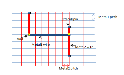
Most of the routers available are grid based routers. There are routing grids defined for the entire layout. Consider it like a graph as below. For grid based routers, there are also preferred routing direction defined for each metal layer. e.g. Metal1 has a preferred direction of “horizontal’, metal2 has preferred routing direction of “vertical’ and so on. So, in the whole layout, metal1 routing grids will be drawn (superimposed) horizontally with metal1 wire picth and metal2 grids will be drawn vertically with metal2 wire pitch between each. You can see that the technology section above has a”pitch” defined for metal1.
`pitch = 0.56`

Routing Grids
The first figure on left figure shows how routing grids are drawn. I am only considering two metals for now, but in a process with more metals, similar grids will be superimposed on the layout for all available metals. Pitch is calculated by determining the minimum spacing required between grid lines of same metal. This can be the minimum spacing of the metal itself, but is usually a value greater than the minimum spacing. This is calculated by taking into account the via dimension as well, so that no two adjacent wires on the grid create any DRC violation even when there are vias present.

Grid based routing with two metals
In a grid based routing algorithm, the router switches the metal as per preferred direction to interconnect the nodes. As you can see in the second figure, metal1 & metal2 wires are drawn along the metal1 & metal2 grids respectively. They are interconnected by via1 to complete the routing path.
Let’s see some more routing related terms.
Global & Detail Routing
The PnR tools you use may let you do routing in various stages, like global routing, track assignment and detailed routing. It could also be that all these algorithmic stages are masked from you and you just have a couple of commands to play with. Most PnR tools deal with the routing problem in a two stage approach. In global routing, the tool partitions the design into routing regions. A rough route is determined taking into account the number of tracks available in each region. Routing congestion is also determined at this stage by calculating 1) how many nets should pass through the region; 2) How many routing tracks are available in the region. In detailed routing, global routing results are used to lay the actual wires interconnecting the nodes. Do a man on the routing options command and you can see how much controllability is available to you in each of these stages for the tool of your choice.
Routing Congestion
It is difficult to route a highly congested design. Some not-so congested designs may have pockets of high congestion which will again create routing issues. It is important that the congestion is analysed and fixed before detailed routing. After CTS, the tool can give you a congestion map by a trial route/ global route values. There are commands to check routability which gives you congestion numbers, blocked pins etc, like `check_routability`.
Routing Order
It is recommended that you route sensitive nets like clock before the rest of the signal route. My assumption is that you have completed power routing after the floorplan stage( because that is what I do.). For this discussion I am going with a traditional routing approach and not considering signal integrity issues. Anyway the order of routing is:
- Power routing : Connect the macro and standard cell power pins to the power rings and staps you have created for the design. IR drop
- Clock Routing : We do not want to upset the skew and delay values for the clock net as much as possible. So the clocks are given higher priority in using routing resources and routed prior to any other net routing. Clock routing can be limited to higher metal layers for reduced RC numbers.
- Signal Routing : The rest of the nets are routed. We can also route groups of nets, and non-default routing rules can also be applied to select nets.
An Example: ICCompiler Script for Routing
################ Power Routing ############################
preroute_standard_cells -connect horizontal  -do_not_route_over_macros
verify_pg_nets


################ Clock Routing ############################

set_parameter -module droute -name doAntennaConx -value 4

source -e $ant_rul_file

set_route_options \
 -groute_skew_control true \
 -groute_clock_routing balanced \
 -droute_CTS_nets normal \
 -same_net_notch check_and_fix \
 -fat_wire_check merge_then_check \
 -merge_fat_wire_on preroute_signal \
 -fat_blockage_as fat_wire

set_route_zrt_common_options -concurrent_redundant_via_mode insert_at_high_cost

route_zrt_clock_tree


################ Signal Routing############################

set_route_zrt_detail_options -port_antenna_mode jump
check_routeability


route_opt
See the ant_rule_file that is sourced into the tool? Antenna Violations and rules will be explained in the next article.
Signal Integrity, EM rules, Antenna and reliability rules, Post Route optimizations etc also are important in today’s designs to meet design and manufacturing objectives. However, this is a pretty good starting point to start tackling each of these aspects one by one.
Hi,
Please elaborate, why we do route clock-nets prior to signal-net? How it is beneficial?
Thanks,
Uttam
For your synchornous design, the clock signals define its behaviour. The clock should be synchronous across all sinks, and to meet this, the routing delay is also taken into consideration. To make sure we do not upset the synchornous nature of the clock, priority is given in routing. There may also be special width, spacing and metal layer rules for clock, which is easier to accomplish when routing resources are relatively high.
See http://vlsi.pro/physical-design-flow-iiiclock-tree-synthesis/
Routing tool vendors talk a lot about DFM capabilities in their routers. What are the really important capabilities and future needs? We want to pick a routing tool that could adapt to future DFM needs with relative ease.
You would want to make sure at least the below capabilities are present, as those are very commonly required
» Redundant via Insertion – to avoid via failures
» Antenna Fixing – to avoid device failures due to charge collection
Also, the below features are desirable
» Metal Density Control
» Litho-aware Routing – increases printability
» Shielding
Tools are rule based, so process maturity affects how efficient the tool is. A mature process will have better results.
Can SPEF file be used for back annotation…Is there any command in cadence where i can back annotate SPEF file and perform routing …else can u give me an idea about how to do backannotation…
Thanks in advance
Use the command read_parasitics to read in the SPEF and then perform optimizations.
You will have to specify -rc_corner if using MMMC flow.
hi sini,
what is track overloading?if track overload happen what is next step to do in lower nodes?
hi sini,
if design have lot of shots and opens then how to extract spef file from starRC tool?
regards,
v.naveen
Can U plze describe about various metal layers present in an IC that we should consider while routing?
Designer usually gives you the number of layers to used also called Stack. Higher the # of layers higher the cost to manufacture.
For example let us consider the # of layers as 7. Then
— Top metal layers (7,6) are typically used for routing clock and PG(Power/Ground) nets because the area of these layers is less when compared to the others.
— Between two metal layers there is one dielectric which is the cut layer.
i have two macros placed side by side with minimum spacing, lets say tile level size is vertically 3mm and horizontally 1mm and pins between these two macros are around 10, i am facing routing congestion at between two macros.
what are the possible causes for routing congestion between two macros. two macros are placed vertically (like two refrigerators side by side).
Are there cells placed on above and below these macros? Select one net, and see where the routes go. If there are cells placed in the channel, add a blockage if that’s causing it.
Maybe to avoid the congestion the macros need to be flipped?
Also, check this link
http://vlsibasic.blogspot.com/2015/08/how-to-decide-on-minimum-spaceing.html
Hi Sini, I am very big fan of your blog.
I have small query.
Let us take Metal1, Via1, Contact.
What is difference between these three in terms of their material properties? Are they all same? or diff? How we will choose particular material to metal and via and contact?
I am not quite sure. I have read somewhere tungsten is used for vias. Aluminium is the typical metal used, and there could be Cu as well. Some technologies have mostly aluminium wires, with a couple of Cu metal layers.
Question 1: In any design two scenarios are there
A. Skew is 200Ps and insertion delay is 600Ps
B. Skew is 300Ps and insertion delay is 500Ps
Both the cases setup and hold are meeting and also tergated skew also meeting then which one will you prefer and why???????
I will go with:
B. Skew is 300Ps and insertion delay is 500Ps
Reason is that, if you have less deeper clock tree, you have less problems with the following:
– OCV
– Dynamic switching power
Question 2: How Scan chin reordering can solve Hold violation????
Hello ,
For a particular design running in ICC2 i am getting this error.Error: worst hold violation exceeds 2000 times nominal buffer delays of * (ns). Design setup issue? Skip hold optimization.What may be the reason for this?
Please run a report_timing -early and see the worst path. You might be able to debug the cause.
why would we only use higher metal layers for power and ground rails.
for example for a design we can use upto 8 metal layers, then why will we use metal8 and metal7 for power and ground rails???
Higher metal layers have:
– Low resistance & good conductivity
– More width can be selected for PG routes compared to lower layers
can you tell me about the couse of voilation like open and short after the routing
When global connections are not proper in the design open occurs.
How can i find out the exact location of all IOpins sitting at core boundary through command mode in cadence tool ?
If i want to route certain inputs of instances using higher metal layers is applying routing blockage to that instance a good idea? Will it be of any use provided the fact that all pins of this particular instance will be in metal 1 layer and vias will be dropped subsequently? this type of requirement is for post-mask ecos
It will only be useful if you have spare cells that have pins that have been brought out on higher level. I am assuming you want to save cost by limiting the number of metals you change.
Hi,
I want to route inputs of particular instances to top routing layer. Is using routing blockages advisable in this case. How can I make sure that routing is always in top layer? I require this specification for post-mask eco
You can limit the layers you modify by freezing the rest of the routing layers. But as mentioned, post mask ecos won’t be easy unless you have made provision for such routing earlier.
Why we are using metal 5 for routing
the ioports and why not any other
Hello Sini,
I have one question with the grid based routing. Does the tool really create grids of Metal1 and Metal2? Or is it just an assumption for the tool and then the tool will start routing the based on the grids of Metal1 and Metal2.