STA - Setup and Hold Time Analysis
It is easy to get confused with the definitions of setup and hold violations. We are used to the definitions of setup and hold times for a single flipflop. The setup and hold violation checks done by STA tools are slightly different. PT aptly calls them max and min delay analysis. However, the other terminology is more common.
First a recap of the setup and hold time requirement of a flipflop.
Setup time is the minimum amount of time the data signal should be held steady before the clock event so that the data are reliably sampled by the clock. Hold time is the minimum amount of time the data signal should be held steady after the clock event so that the data are reliably sampled.
Setup Analysis (Max Delay Analysis)
Now, let us see what is meant by setup analysis for a timing path. Timing paths can be the following types:
1. Input port to a D pin of Flop. 2. CLK pin of Flop1 to D pin of Flop2 3. Q pin of flop to an output port 4. Input to output port through purely combinational logic.
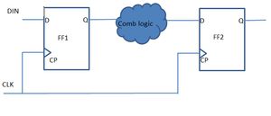
We will take up a register to register path (2 above) for explanation.
[caption id="attachment_1034" align="alignright" width="300"] Register to register path[/caption]
We need to define some terms now. Consider the same clock goes to both FF1 & FF2. CLK is fed to both FF1&FF2. At clock edge A, FF1 is launching the data. That is, the D value causes a change in Q of FF1. So we call FF1 as lauching flop for this timing path. This signal will be captured at FF2 after one cycle.(For a single cycle path). So FF2 becomes our capturing flop, and clock edge B becomes our _capturing edg_e. [caption id="attachment_1036" align="alignleft" width="300"] Launch and Capture Edges[/caption]
For ease of understanding, let us decide every component in the circuit is ideal. i.e. the flipflops have no setup and hold time requirements and clock is ideal. ie, CLK arrives at CP of FF1 & FF2 at 0 delay, edges coinciding.
The data path of the timing circuit is through CP of FF1 to D of FF2. Now let us calculate the delay encountered by data and clock while reaching FF2.
Data path delay CLK->Q delay of FF1 + Comb path delay In analysis, we call this the Arrival Time.
Clock path delay 0. (ideal clock)
However, we are checking the setup at the clock edge B. So we need to add one clock cycle to the clock path delay to get the Required Time.
Required Time = Clock period.
Data launched at FF1/CP should arrive at FF2/D in one clock period. So in setup check, we say a violation has occured if the data path delay is more than one clock cycle.
Now, let us increase the complication.
Clock has insertion delays. So the actual datapath delay is: CLK delay till FF1/CP + CLK->Q delay of FF1 + Comb path delay
And the actual clock path delay is: CLK delay till FF2/CP. Required Time = Clock period + CLK delay till FF2/CP.
Now, we should also take into account the setup requirement of FF2. ie. Data at FF2/D should be stable for at least TsFF2 before the clock edge. So the required time for data arrival at FF2/D is Clock period + CLK delay till FF2/CP- TsFF2 .If data arrives later than the clock path delay calculated above, the data won't be captured at edge B.
From above, it is clear that setup analysis checks for the maximum allowable delay for the timing path.
Hold Analysis (Min Delay Analysis)
Now let us move on to Hold analysis.
Let us take the same timing path above. Here you are verifying that the data is not captured at FF2/D on launching edge A of the CLK. ie. it is checking for the minimum delay the data should take to arrive at the second flop for the circuit to function correctly.
[caption id="attachment_1047" align="alignleft" width="300"] Timing Analysis with ideal clock[/caption]
ThFF2 is the library hold time value of flop FF2. If the Data launched by FF1 reaches D of FF2 fast enough, it may be captured at the same clock edge A by the flop FF2. Hence the minimum delay requirement for the timing path is that the path to D should at least take more time than the hold time requirement of the flop FF2, so as not to corrupt the data. (Look up the .lib file for the hold time values for pin D relative to clcok pin CP of the flip flop type of FF2).
In simple terms, this makes sure the launched data does not arrive at the capture point too soon. Data launched from launching flop is allowed to arrive at the input of the second flop only after a delay greater than its hold requirement so that it is properly captured.
With clock delays in place, data path delay is CLK delay till FF1/CP + CLK->Q delay of FF1 + Comb path delay Arrival time = CLK delay till FF1/CP + CLK->Q delay of FF1 + Comb path delay Clock path delay is CLK delay till FF2/CP. Required Time = CLK delay till FF2/CP + Hold requirement of FF2
Note that we are no longer adding the clock period to the required time. This is because the hold is checked with the same clock edge, and setup with the next clock edge.
From the figure above,assuming ideal clock, there is a window of time which is between the minimum required(ThFF2) and the maximum allowed(Clock period - TsFF2) that the timing path can correctly have. If the data path takes less time that ThFF2, we say a hold violation has occurred. If the data path takes more time than Clockperiod-TsFF2, we say a setup violation has occurred.
Take a timing report and draw the clock and data path diagrams to understand this further.