Intrinsic and Extrinsic Semiconductors
Last modified 2020-01-09
Sini
A semiconductor material in its pure form is called an intrinsic semiconductor. To be classified thus, its impurity content should be less than 1 part in 100 million parts of semiconductor. As we mentioned earlier, Si or Ge has a crystal lattice where electrons are shared between surrounding atoms.

An intrinsic semiconductor acts as an insulator at absolute zero. As temperature increases some electrons gain enough energy to jump to the conduction band and become free electrons. A hole is generated when an electron breaks free from the covalent bond, and the unpaired electron in the bond will try to acquire an electron to form the bond whenever it can. As a result, it appears that the quasiparticle hole travels randomly along the lattice.
Drift Current
If we were to connect a battery across a semiconductor, the electrons and holes travel towards the positive and negative terminals of the battery respectively.

Due to the movement of electrons and holes, now there is a net current in the direction of hole flow. This is called the drift current.
Extrinsic Semiconductors
When impurities are intentionally added to semiconductor materials, they are called extrinsic semiconductors. Most semiconductor devices are made by these types of materials, as the properties of the semiconductors can be greatly varied by the impurities added. The process of adding impurities in a controlled manner to a semiconductor is called doping. There are two types of extrinsic semiconductors depending on the impurities added.
-
N-type Semiconductor
Si or Ge has four electrons in their valence shell. Group V elements of the period table are pentavalent, i.e. they have five electrons in their valence shell. Let us consider what happens when a pentavalent impurity like phosphorous is introduced to pure Si lattice. An impurity atom replaces one Si in the lattice.
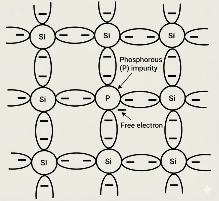
Four electrons in the valence shell of Phosphorous forms covalent bonds with the neighbouring four atoms of Si. However, there is another electron in the valence shell of P that cannot form a covalent bond in the lattice. This excess electron is far from the nucleus and can easily jump to conduction band with a very small amount of energy. In fact at room temperature all the excess electrons becomes free electrons. For such a doped material, there will also be the thermally generated electron-hole pairs and the electrons donated by the pentavalent impurities. Thermally generated electron-hole are equal in number, but the excess electrons provided by the impurity atoms mean that the majority carriers is such a semiconductor is electrons. Such semiconductors are called N-type semiconductors.
-
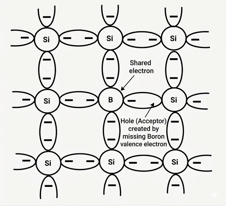
P-type Semiconductor If a trivalent impurity like Boron is used for doping pure semiconductor crystal like Si, the resultant material is called a P-type semiconductor.