ASIC Physical Design Flow
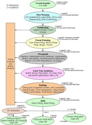
In the VLSI design cycle, after the circuit representation is complete, we go to “physical design”. This is the stage where the circuit description is transformed into a physical layout, that is the actual physical representation of the circuit in terms cells, their placement, power connections and the interconnection between them. I am consolidating the previous design flow articles in this website here.
By Renoy - Own work, Public Domain
- Netlist In & Floorplanning: https://vlsi.pro/physical-design-flow-i-netlistin-floorplanning/
- Placement : https://vlsi.pro/physical-design-flow-ii-placement/
- Clock Tree Synthesis : https://vlsi.pro/physical-design-flow-iiiclock-tree-synthesis/
- Routing: https://vlsi.pro/physical-design-flow-iv-routing/
- Physical Verification: https://vlsi.pro/physical-design-flow-v-physical-verification/