Power Dissipation: Leakage Power
Part 1: Sources of Leakage
Reduction of power consumption is a requirement for semiconductor devices. First let us list the sources of power to understand how to go about reducing it.
Two power components of a CMOS circuit are:
- Static Power
- Dynamic Power
Static power is the power consumed while the circuit is inactive or idle. i.e. all inputs are at held valid levels, there is no switching activity and and the circuit is not charging. However even in this `steady state`, there are some leakage currents in the device which contribute to the leakage power. This power dissipation doesn't depend on input conditions or load capacitance, but is dependent on the device.
There are many different contributing factors to leakage as mentioned below.
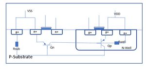
- PN-junction current We had discussed the parasitic p-n junctions fromed in the CMOS device in post vlsi.pro/cmos-latchup/. Even when the p-n junctions are reverse-biased, there is a small current flowing through these junctions due to minority carriers.When the temperature increases, the minority carrier injection also raises, and causes an increase in leakage current.
 [su_spacer size="10"]
 - Sub-threshold current When the transistor is in off state, i.e. when the gate-to-source voltage is less than the threshold voltage, there is a leakage current from drain to source which is called the subthreshold current.This current is highest when the gate voltage is just below the threshold voltage, as as voltages have scaled down with technology, this is becoming a major component of leakage power in semiconductor devices.
 [su_spacer size="10"]
 - Thin oxide gate tunneling As transistor geometries reduce, gate oxide thickness have also been reducing enabling higher performance. However, this thinning of oxide layer causes leakage current between substrate and gate through the oxide.
 [su_spacer size="10"]
 - Drain induced barrier lowering (DIBL) This is a short channel effect. When Vds and Vgs are 0V, there is no flow of current from source to drain. However, with shorter channels, the drain voltage will effectively lower this potential barrier. The depletion region formed by the drain voltage is close enough to the source and can help in turning on the device with a lower Vgs, effectively lowering the threshold voltage.
 [su_spacer size="10"]
 - Hot carrier injection