Physical Design Flow IV:Routing

I. NetlistIn & Floorplan II. Placement III. Clock Tree Synthesis
After CTS, the routing process determines the precise paths for interconnections. This includes the standard cell and macro pins, the pins on the block boundary or pads at the chip boundary. After placement and CTS,the tool has information about the exact locations of blocks, pins of blocks, and I/O pads at chip boundaries. The logical connectivity as defined by the netlist is also available to the tool. In routing stage, metal and vias are used to create the electrical connection in layout so as to complete all connections defined by the netlist. Now, to do the actual interconnections, the tool relies on some "Design Rules". It is essential that
- Tool completes all connections that are defined by the netlist (100% routability), i.e. no LVS errors.
- No design rules are violated in completing the routes(No DRC errors).
- All timing constraints are met.
Process Design Rules
If you refer to Physical Design Flow I, an input to the PnR tool is a 'Technology File' (or technology LEF for Cadence.) These are the constraints that the router should honour.
An example for technology file rules for metal1 & via1 are given below.
Layer "M1" { layerNumber = 10 maskName = "metal1" pitch = 0.56 defaultWidth = 0.24 minWidth = 0.24 minSpacing = 0.24 fatWireThreshold = 10 }
Layer "VIA1" { layerNumber = 11 maskName = "via1" pitch = 0 defaultWidth = 0.24 minWidth = 0.24 minSpacing = 0.24 }
ContactCode "via1" { contactCodeNumber = 1 cutLayer = "VIA1" lowerLayer = "M1" upperLayer = "M2" isDefaultContact = 1 cutWidth = 0.24 cutHeight = 0.24 upperLayerEncWidth = 0.01 upperLayerEncHeight = 0.06 lowerLayerEncWidth = 0.06 lowerLayerEncHeight = 0.01 minCutSpacing = 0.24 }
Your techfile will have many more parameters for each layer. As you can see, for M1 above, minimum spacing, minimum width, minimum area etc are defined. It also specifies which via connects the two metal layers M1 & M2. If any of these parameters like spacing, width, via size etc are violated for any routing the tool does, you will get a DRC error.
Routing Grids
Most of the routers available are grid based routers. There are routing grids defined for the entire layout. Consider it like a graph as below. For grid based routers, there are also preferred routing direction defined for each metal layer. e.g. Metal1 has a preferred direction of "horizontal', metal2 has preferred routing direction of "vertical' and so on. So, in the whole layout, metal1 routing grids will be drawn (superimposed) horizontally with metal1 wire picth and metal2 grids will be drawn vertically with metal2 wire pitch between each. You can see that the technology section above has a"pitch" defined for metal1. `pitch = 0.56`
[caption id="attachment_645" align="alignleft" width="300"] Routing Grids[/caption]
The first figure on left figure shows how routing grids are drawn. I am only considering two metals for now, but in a process with more metals, similar grids will be superimposed on the layout for all available metals. Pitch is calculated by determining the minimum spacing required between grid lines of same metal. This can be the minimum spacing of the metal itself, but is usually a value greater than the minimum spacing. This is calculated by taking into account the via dimension as well, so that no two adjacent wires on the grid create any DRC violation even when there are vias present.
[caption id="attachment_646" align="alignleft" width="300"]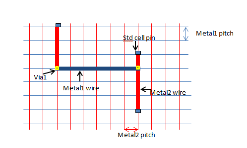 Grid based routing with two metals[/caption]
In a grid based routing algorithm, the router switches the metal as per preferred direction to interconnect the nodes. As you can see in the second figure, metal1 & metal2 wires are drawn along the metal1 & metal2 grids respectively. They are interconnected by via1 to complete the routing path.
Let's see some more routing related terms.
Global & Detail Routing
The PnR tools you use may let you do routing in various stages, like global routing, track assignment and detailed routing. It could also be that all these algorithmic stages are masked from you and you just have a couple of commands to play with. Most PnR tools deal with the routing problem in a two stage approach. In global routing, the tool partitions the design into routing regions. A rough route is determined taking into account the number of tracks available in each region. Routing congestion is also determined at this stage by calculating 1) how many nets should pass through the region; 2) How many routing tracks are available in the region. In detailed routing, global routing results are used to lay the actual wires interconnecting the nodes. Do a man on the routing options command and you can see how much controllability is available to you in each of these stages for the tool of your choice.
Routing Congestion
It is difficult to route a highly congested design. Some not-so congested designs may have pockets of high congestion which will again create routing issues. It is important that the congestion is analysed and fixed before detailed routing. After CTS, the tool can give you a congestion map by a trial route/ global route values. There are commands to check routability which gives you congestion numbers, blocked pins etc, like `check_routability`.
Routing Order
It is recommended that you route sensitive nets like clock before the rest of the signal route. My assumption is that you have completed power routing after the floorplan stage( because that is what I do.). For this discussion I am going with a traditional routing approach and not considering signal integrity issues. Anyway the order of routing is:
- Power routing : Connect the macro and standard cell power pins to the power rings and staps you have created for the design. IR drop
- Clock Routing : We do not want to upset the skew and delay values for the clock net as much as possible. So the clocks are given higher priority in using routing resources and routed prior to any other net routing. Clock routing can be limited to higher metal layers for reduced RC numbers.
- Signal Routing : The rest of the nets are routed. We can also route groups of nets, and non-default routing rules can also be applied to select nets.
An Example: ICCompiler Script for Routing
################ Power Routing ############################ preroute_standard_cells -connect horizontal -do_not_route_over_macros verify_pg_nets
################ Clock Routing ############################
set_parameter -module droute -name doAntennaConx -value 4
source -e $ant_rul_file
set_route_options \ -groute_skew_control true \ -groute_clock_routing balanced \ -droute_CTS_nets normal \ -same_net_notch check_and_fix \ -fat_wire_check merge_then_check \ -merge_fat_wire_on preroute_signal \ -fat_blockage_as fat_wire
set_route_zrt_common_options -concurrent_redundant_via_mode insert_at_high_cost
route_zrt_clock_tree
################ Signal Routing############################
set_route_zrt_detail_options -port_antenna_mode jump check_routeability
route_opt
See the ant_rule_file that is sourced into the tool? Antenna Violations and rules will be explained in the next article.
Signal Integrity, EM rules, Antenna and reliability rules, Post Route optimizations etc also are important in today's designs to meet design and manufacturing objectives. However, this is a pretty good starting point to start tackling each of these aspects one by one.