Physical Design Flow V: Physical Verification

I. NetlistIn & Floorplan
II. Placement
III. Clock Tree Synthesis
IV. Routing

After routing, your layout is complete. Now a number of checks are performed to verify that the drawn layout works as intended.

  1. Physical verification
  2. Equivalence Checking
  3. Timing Analysis

Equivalence check will compare the netlist we started out with (pre-layout/synthesis netlist) to the netlist written out by the tool after PnR(postlayout netlist).Physical verification will verify that the post-layout netlist and the layout are equivalent. i.e. all connections specified in the netlist is present in the layout.This article explains physical verification.

Physical Verification

After routing, your PnR tool should give you zero DRC/LVS violations. However, the PnR tool deals with abstracts like FRAM or LEF views. We use dedicated physical verification tools for signoff LVS and DRC checks. Some of these are Hercules from Synopsys, Assura from Cadence and Calibre from MentorGraphics.

The major checks are:

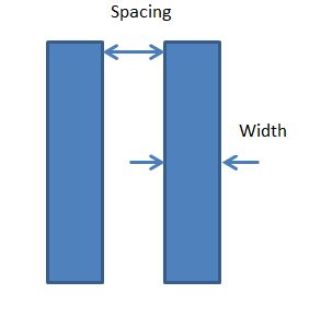
  1. DRC
    DRC checks determine if the layout satisfies a set of rules required for manufacturing. The most common of these are spacing rules between metals, minimum width rules, via rules etc.There will also be specific rules pertaining to your technology. An input to the design rule tool is a ‘design rule file’ (called a runset by Synopsys’ hercules). The design rules ensure sufficient margins to correctly define the geometries without any connectivity issues due to proximity in the semiconductor manufacturing processes, so as to ensure that most of the parts work correctly. The minumum width rules exists for all mask layers, and spacing between the same layers are also specified. Spacing rules may change depending on the width of one or both of the layers as well. There can also be rules between two different layers, and specific via density rules etc. If the design rules are violated, the chip may not be functional.
    Spacing & Width checks

    DRC – Spacing & Width checks

    DRC checking software, like Assura, Hercules or Calibre usually takes the layout in any of the supported formats, like GDSII.

  2. LVS

    LVS is another major check in the physical verification stage. Here you are verifying that the layout you have created is functionally the same as the schematic/netlist of the design-that you have correctly transferred into geometries your intent while creating the design. So all the connections should be proper and there shouldn’t any missing connections etc.

    The LVS tool creates a layout netlist, by extracting the geometries. This layout netlist is compared with the schematic netlist. The tool may require some steps to create either of these netlists(e.g. nettran run in synopsys)
    If the two netlists match, we get an LVS clean result. Else the tool reports the mismatch and the component and location of the mismatch. Along with formal verification, which verifies if your pre-layout netlist matches the post-layout netlist,LVS verifies the correctness of the layout w.r.t intended functionality.

    Some of the LVS errors are:

    • Shorts – Wires that should not be connected are overlapping.
    • Opens – Connections are not complete for certain nets.
    • Parameter mismatch – LVS also checks for parameter mismatches. e.g. It may match a resistor in both layout and schematic, but the resistor values may be different. This will be reported as a parameter mismatch.
    • Unbound pins – If the pins don’t have a geometry, but all the connection to the net are made, and unbound pin is reported.
  3. Antenna
  4. Process antenna effect or “plasma induced gate oxide damage” is a manufacturing effect. i.e. this is a type of failure that can occur solely at the manufacturing stage. This is a gate damage that can occur due to charge accumulation on metals and discharge to a gate through gate oxide.

    Let us see how this happens. In the manufacturing process, metals are built layer by layer. i.e. metal1 is deposited first, then all unwanted portions are etched away, with plasma etching. The metal geometries when they are exposed to plasma can collect charge from it. Once metal1 is completed, via1 is built, then metal2 and so on. So with each passing stage, the metal geometries can build up static electricity. The larger the metal area that is exposed to the plasma, the more charge they can collect. If the charge collected is large enough to cause current to flow to the gate, this can cause damage to the gate oxide. This happens because since the layers are built one-by-one, a source/drain implant may not be available for discharge as in fig.b.

    Process Antenna

    Process Antenna

    Antenna rules are normally expressed as an allowable ratio of metal area to gate area. Each foundry sets a maximum allowable antenna ratio for its processes. If the metal area–which is cumulative, i.e. the sum of the ratios of all lower layer interconnects in addition to the layer in check–is greater than the allowable area, the physical verification tool flags an error.For example, let’s say maximum allowable antenna ratio for metal1 is 400. If the gate area is 1 sq.u and if the metal area connecting to the gate is 500 sq.u, there will be a process antenna violation.

  5. ERC
    ERC (Electrical rule check) involves checking a design for all electrical connections that are considered dangerous.

    • Floating gate error – If any gate is unconnected, this could lead to leakage issues.
    • VDD/VSS errors – The well geometries need to be connected to power/Ground and if the PG connection is not complete or if the pins are not defined, the whole layout can report errors like “NWELL not connected to VDD.

47 comments on “Physical Design Flow V: Physical Verification

    1. Sini Mukundan Post author

      I have only run package DRC. It checks the rules when your IC is connected by wires to the package you have selected. Checks for minimum and maximum wire length from package pin to a pad, distance between two adjacent wires etc. I would assume package LVs to be similar,checking for LVS rules.

      Reply
    1. Sini Mukundan Post author

      I am assuming you are getting this in Assura?
      If you did the layout in EDI, make sure you have a terminal for VDD. If not create one using

      createPGPin -geom   VDD

      before writing out the design.

      You can also edit this in ICFB. You can use “create pin from labels”.

      Reply
      1. pramod

        Why we use Higher metal layers for power and ground routing. In my project i am using m6 for P/G connections. How can they have less sheet resistance. I see the same width and resistance for all the metal layers in my library. Please explain it

        Reply
        1. Sini

          Sheet resistance also depends on thickness. http://www.ece.gatech.edu/research/labs/vc/theory/sheetRes.html

          Check you technology files for all the metals’ values. Also, your design rule document should have the information. (Am not sure why a technology has all the same RC characteristic for all metals.) If you are using Cadence LEF, these are present in tech_lef.

          RESISTANCE RPERSQ 0.058 ;
          CAPACITANCE CPERSQDIST 1.35e-05 ;
          HEIGHT 2.5 ;
          THICKNESS 0.54 ;

          Reply
  1. CLR

    Hey we are getting antenna violation on macros and we are restricted to use only till metal 5 and violation is occurring in metal 5 , since the violation is occuring on metal 5 we are not able to use metal jogging technique and we had to continue with antenna diodes insertion and we don’t know how proceed… Should we add diodes manually and connect it or is there any other way out? Please revert back . Thank you.

    Reply
    1. Sini Mukundan Post author

      Do you mean it is coming to the pins of the hard macro inside your block? Then you might have to add diodes manually. You can write a script to add these to all offending pins.

      If the macro is your block, then you can still jump metal even if the violation is on top metal. Just make sure it is very close to the offending gate.The tool should have fixed the majority of violations in that case. Check you routing options, and see if all the relevant fix options are turned on and the antenna values in tech file is correct. If you have a larger diode in the library, use it for your route iterations.

      Reply
  2. CLR

    HI
    while Physical verification i’m getting some DRC violations like 90 degree gates are not allowed for thin gate and some violations regarding via shapes
    should it be fixed manually or is there a automation in tool

    Reply
  3. Naveen Reddy

    Hi Sini,
    What is halo cell internal diagram? why we are using rather than dcap,endcap,filler cells.

    Reply
    1. Sini Mukundan Post author

      When I refer to halo, it is the placement keepout margin around macros. Essentially a placement blockage.

      Maybe you use the term for some other kind of cells in your flow. It is not a generic cell type as far as I know.

      Reply
  4. sandeep

    Hi Mam,
    Thanks for all the information you have been providing on the website, really appreciate your effort.
    I want to understand why at all there is a min/max width rule specified for metal layers. What is the underlying purpose?

    Reply
    1. karnakar reddy

      Min width are rules are used, to make sure that metal is manufactured correctly to provide intended functionality, i.e., while manufacturing we may not get the metal widths as we expected , simply , at any critical conditions to get proper connectivity we use min width violation rules

      Reply
  5. Arif

    If in the top metal layer we get a antenna violation and we do not have any antenna diode available then how to solve the violation??????

    Reply
    1. karnakar reddy

      can solve by changing the stack of metal . for example you got violation on M9 and it is the top most layer then if possible any where break the metal and connect to M8 then V8 to M9 . there metal will be broken and no need to waste space by adding buffers.

      Reply
  6. Arif

    Question: While doing synthesis,
    a. Unused logic and ports are removed while optimization If we specify so
    b. Unused logic is removed Normally
    c. Unused logic is untouched

    Reply
  7. Kashyap Shah

    Hello,
    The article was really helpful. The project that I am working on are having timing violations on working. So, can you please guide regarding how can I close the timing after routing or how can I fix the setup and hold timing after routing?

    Reply
    1. Sini Mukundan Post author

      Kashyap,

      If the tool was unable to meet it on its own after postroute optimizations, you need to analyse your timing reports. This has to be design specific OR due to your SDC constraints.

      Reply
  8. Rinu Johnson

    Hi

    Any library checks need to be done by the end of the PD flow apart from DRC and LVS check…??? Thanks in advance

    Reply
    1. Sini Mukundan Post author

      I haven’t seen a single site for that, but if you google your query it will usually throw up a lot of articles.

      I believe most of my colleagues refer ‘the art of analog layout’ by Alan Hastings.

      Reply
  9. SKG

    Hi,

    I have a small question on LVS. Was not completely sure why open nets occur in the design and what is the reason for that?

    Reply
    1. karnakar reddy

      while routing if congestion is there in metals , the tool can’t handle and it will left the nets half-routed.

      Reply
  10. K .P.MANJUNATH

    hello madam can we prooceed in there is any timing violations in the netlist provided after the synthesis report and if we procced on which basis we will proceed

    Reply
    1. Sini Mukundan Post author

      I forgot the specific commands but the antenna diodes need to be specified in milkyway library. (Maybe CLF/command)

      e.g.
      If you were using LEF file, you will have the following..

      MACRO adiode1
          CLASS CORE ANTENNACELL ;
      
      Reply
  11. kalyan

    Dear mam…I’m doing my internship here in ARICENT in PD domain so i would like to know in what way i can make use of this internship to get job as well(They said at the end of the internship based on performance they will hire me),so please sir any suggestions?

    Reply
  12. AKASH SHARMA

    hello mam,
    can we use same metal layer like M6 for all the connection like clock routing,signal rounting etc ? pls mention the reason of your answer.
    Thanks in advance.

    Reply
  13. Naresh Marikanti

    hi i am naresh i am interested in physical design i am Mtech graduate i am training in pd in hyd one institute please guide me i need your suggestions
    thank you

    Reply

Leave a Reply

Your email address will not be published. Required fields are marked *