Physical Only Cells; Well Taps & Decap Cells

In PD flow, you must have come across the term physical only cells. Let us explore a few of them. Well Tap Cells Decap Cells **Filler Cells
Well Tap Cells
Library cells usually have well taps which are traditionally used so that your n-well is connected to VDD and substrate is connected to GND. In the CMOS cross-section we discussed earlier in CMOS latch up, we can see the Bulk (B) contacts for PMOS and NMOS.

Digital library cells usually have taps inside them, as given in the above layout. However, each and every CMOS device need not have these taps. Theoretically, we need only one VDD tap per NWELL (standard cell row), and a single substrate connection. If we remove the well ties from the above layout, we get a significant area reduction. We now have "tap-less" libraries, where not every cell has these in-built tap connections. Instead a WellTap cell is provided which has only the well-ties to VDD/GND inside them.  However, having only single nwell/substrate tap in a row can lead to Latch up due to high well and substrate resistance. Typically there is a design rule that for certain distance, there should be a tap cell present.
Given above is an example of a ‘checker-board’ pattern for ensuring design rule compliancy. In cadence Innovus, ‘addWellTap’ command can add these cells automatically according to distance and pattern specification.
Decap Cells Decoupling capacitors are another type of physical only cells used in PD flow. These do not have any logical functionality. These cells essentially act as a capacitance between power and ground rails, and hence as a charge reservoir that can be counted upon while there is a high demand for current from the power lines. They can be thought of as localized power supplies within your chip.
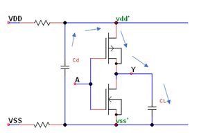
Consider the circuit given below. There is a decoupling capacitor Cd and an iverter.CL is the load seen by the output pin Y of the inverter due to the cells downstream. 
Due to the resistance of the power structure, there is voltage drop (IR drop) and voltage vdd’ seen by the inverter above is less than the power supply VDD. In an inverter operation, say when A is 0, the output capacitor CL is to be at level VDD. It can so happen that due to simultaneous switching of many cells in the rail, the instantaneous voltage drop further degrades the power supply. Depending on the drop, vdd’ can be much lower, close the VOH for ‘high’ state. This reduces the noise handling capability of the circuit due to reduced noise margin, and any surge in power supply can push the circuit to an unknown logic state.
If you have a capacitor between the rails, it acts as a charge reservoir. When the current demand is high, it provides an alternative path which can pull the CL to VDD faster. When the circuit close to it is not drawing current, the capacitor charges back to VDD.
We have a special type of cells called decap fillers which does exactly what is described above. There are decap insertion flows available in today’s tools, which provides the optimum placement for decap cells in the layout after analyzing power grid and cell density.One drawback of these cells is that it increases the leakage power of your chip.**